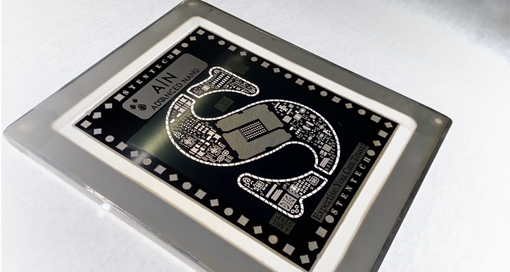


Our award winning coating technology
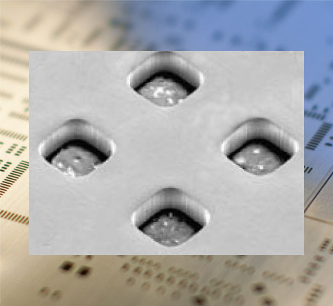
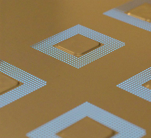
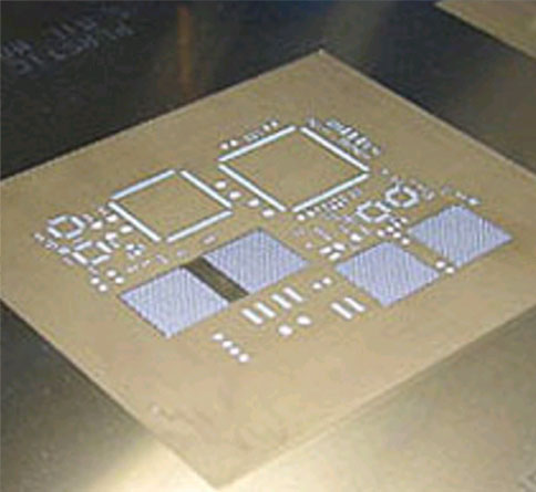
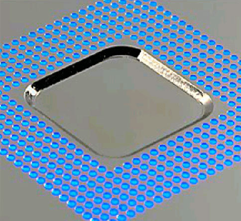
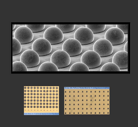
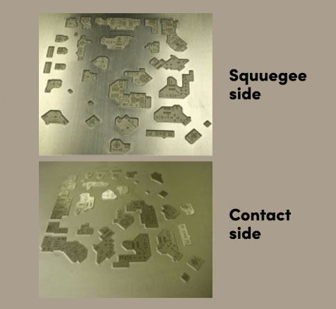
StenTech's award winning Advanced Nano is an exceptional coating that revolutionizes stencil technology. Unlike traditional stencils, this highly unique coating is applied to the bottom side of the stencil and inside the apertures, leaving the squeegee side uncoated. This advanced coating grants the stencil remarkable anti-adhesion properties, preventing solder flux from sticking to it. Utilizing a specialized 1-2 um hardened nano coating, Stentech's Advanced Nano stencil boasts a permanent hydrophobic layer that repels solder flux.
Consequently, this innovative feature facilitates enhanced paste transfer during printing processes, leading to improved efficiency and precision in electronic manufacturing. Most of all it allows SAME DAY DELIVERY of your stencils.
Read More